説明
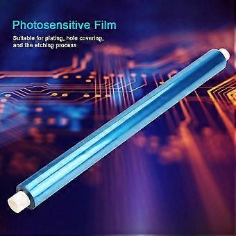
Resolution PCB Photosensitive Film with Adhesion for Etching and Plating
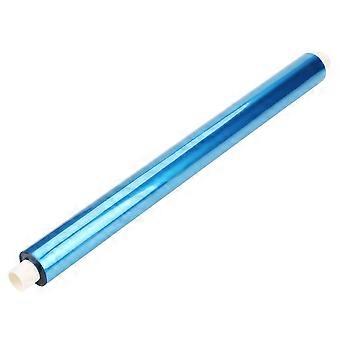
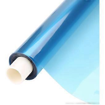
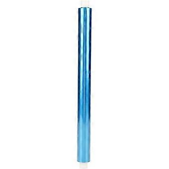
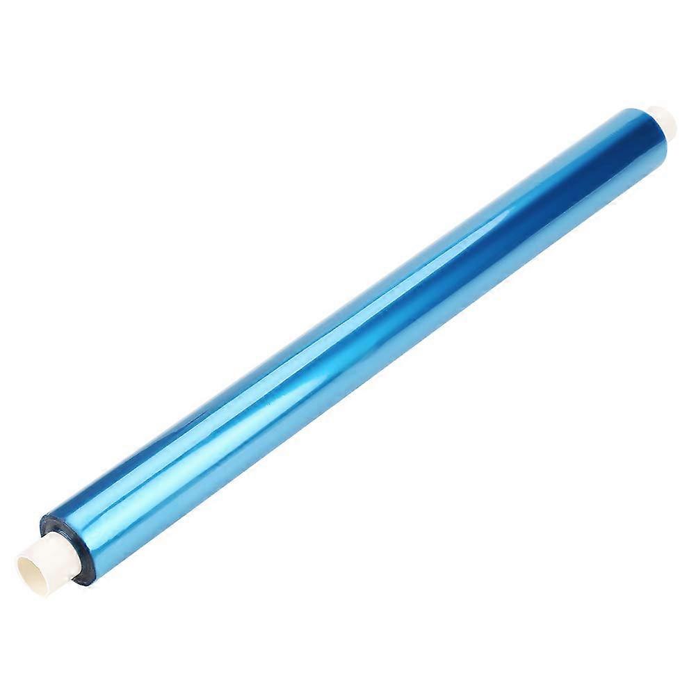
Photosensitive Photographic Film for PCB Production — 30 cm x 500 cm, plastic material
Key benefits
Accurate pattern transfer: Stick the photosensitive film directly onto the PCB to create a sensitive, exposureready mask that produces clear images after exposure, reducing alignment errors and rework.
Multistep process support: Designed for plating masks, hole covering, and etching, so one film handles the common steps in PCB fabrication without switching materials.
Long, consistent roll: The 30 cm x 500 cm size gives a continuous supply for multiple boards or large panels, minimizing joins and seams during production.
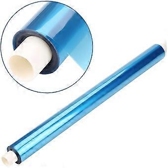
Easy handling and stable performance: Made from a plastic photosensitive material that is easy to apply and maintains dimensional stability during processing.
What it does and how it helps
Functions as a temporary, photosensitive mask that adheres to the PCB surface, allowing precise exposure of circuit patterns.
Improves process reliability by providing a clear, contrast image after exposure, enabling more accurate etching and plating results.
Saves time in smallbatch and prototype workflows by simplifying mask preparation and reducing the need for manual touchups.
Material, size, and compatibility
Material: Photosensitive plastic film suitable for standard PCB exposure and etching workflows.
Size: 30 cm x 500 cm roll for extended use across multiple boards or panels.
Compatibility: Intended for direct application on PCB substrates where plating, hole protection, and etching steps are required.
Practical use scenarios
Prototype development: Apply the film to singleboard prototypes to expose and etch accurate traces without outsourcing masks.
Smallbatch production: Use the long roll to cover multiple small PCBs or a large panel, streamlining plating and holecovering operations.
and modification: Mask specific areas for selective plating or etching during rework or board alteration.
Performance highlights
Produces clear image results after exposure for precise circuit definition.
Suitable for plating, hole covering, and etching applications common in PCB fabrication.
Easy to apply and reliable throughout the exposure and development steps.
Specifications
Product type: Photographic/photosensitive film for PCB production
Material: Plastic photosensitive film
Dimensions: 30 cm x 500 cm
Primary functions: Sticking to PCB surface for exposure, plating, hole covering, etching
Use this photosensitive film when you need a stable, easytoapply masking solution that delivers clear exposure images and supports multiple PCB fabrication steps.
-
Fruugo ID:
458433103-966042642
-
EAN:
6452872679657